PCB Manufacturing Process Steps
Producing printed circuit boards involves a complex procedure that must be carefully executed to ensure optimal performance of the final product. While the fabrication processes for single, double, and multilayer PCBs differ only after the first layer is produced, the number of steps involved in manufacturing can vary significantly depending on the PCB's structure. In fact, some PCBs may require 20 or more steps to be completed. It is crucial not to skip any step or reduce the procedure as doing so could have a detrimental effect on the circuit board's performance. However, if all the steps are completed successfully, the PCBs should function correctly and serve as critical electronic components.
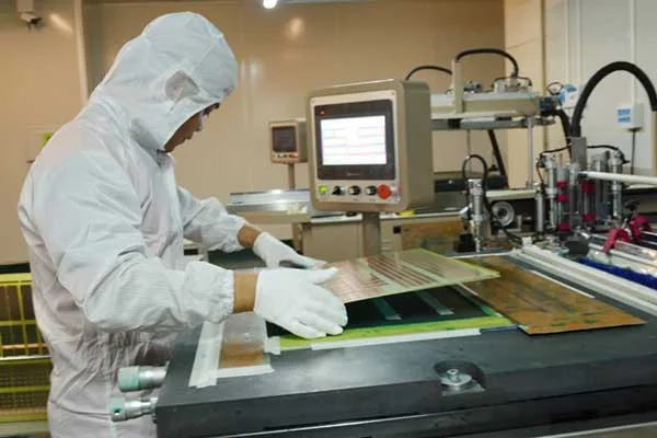
Total Time Needed: 5 days
Required Tools and Equipments:
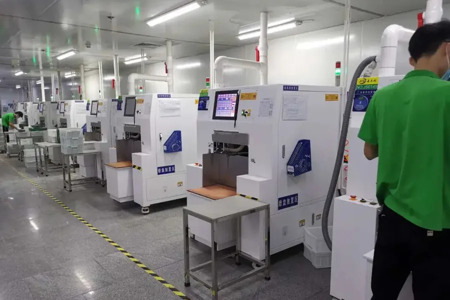
- PCB Material Cutting Machine
- Drilling Machine
- Pattern Plating Line
- PCB PTH LIne
- Strip Film Etching Line
- PCB Multilayer Pressing Equipment
- PCB Solder Mask Expose Machine
- PCB Solder Mask Develop Line
- Solder Mask Screen Silk Print Machine
- PCB Legend Solder Mask Overn
- PCB Pattern Expose Machine
- PCB Pattern Develop Machine
- PCB E-test Machine
- PCB AOI Machine
- V-cut Machine
Materials
- Copper Clad laminate (CCL)
- Films
- Epoxy Resin
- FR-4
- Prepreg
- Copper Foil
PCB Manufacturing Process Step by Step
Step 1 : Design and Output
PCB designs must be compatible with the layout created by the designer using PCB design software, such as Altium Designer, OrCAD, Pads, KiCad, and Eagle. Designers must inform their contract manufacturer of the software version used to avoid issues caused by discrepancies before fabrication.Once the design is approved, designers export the design to the format supported by the manufacturer, typically extended Gerber or IX274X. This format encodes comprehensive information, including copper tracking layers, drill drawings, apertures, and component notations, and undergoes checks by the software to ensure no errors go undetected. Designers examine the plan for track width, board edge spacing, trace and hole spacing, and hole size.After examination, designers send the PCB file to the PC manufacturer for production. Most PCB manufacturer run a Design for Manufacture (DFM) check before fabrication to ensure the design fulfills the requirements for minimum tolerances during the manufacturing process.

Step 2: Pre-Production Engineering
Design Review and Engineering QuestionsTo ensure the quality of the printed circuit board, the design must undergo a thorough review by an engineer to check for any errors or flaws. Once the engineer approves the design, it moves on to the printing phase. The customer-supplied data (gerber) is used to produce manufacturing data, including artworks for imaging processes and drill data for drilling programs. Engineers compare demands and specifications against capabilities to ensure compliance and determine the process steps and checks.

Step 3: From File to Film
PCB printing begins with designers outputting schematic files and manufacturers conducting a DFM check. Using a special printer called a plotter, manufacturers make highly detailed films of the PCB design. The resulting plastic sheets show a photo negative of the PCB, with black ink representing the conductive copper parts and clear areas representing non-conductive material. The films are developed automatically and stored securely to prevent any unwanted contact.Each layer of PCB and solder mask requires its own set of clear and black film sheets, with registration holes punched through all sheets to ensure perfect alignment. The accuracy of the registration holes is achieved by adjusting the table on which the film sits. The Artwork Master, a photographic image of the PCB pattern on film used to produce the circuit board, is a crucial step in PCB production that directly affects the quality of the final product. There are three types of Artwork Master: conductive pattern, solder mask, and silkscreen.

Step 4: Copper Clad Laminate Cutting
PCB production commences with a large sheet of material. However, due to equipment limitations and manufacturing capabilities, the factory imposes specific requirements on the minimum and maximum processing sizes. Consequently, the raw material of the PCB, Copper Clad Laminate, is cut into the appropriate processing size using an automatic cutting machine under the guidance of the manufacturing instruction (MI) prior to production.

Step 5: Printing the Inner Layers
The initial step of the PCB production process is transferring the electronic design to the board surface. This is achieved through the use of an artwork film, photosensitive dry-film, and UV light. The artwork exposes the dry film, which is then polymerized by the UV light. This crucial step is conducted in a controlled clean room environment. The process is known as imaging, whereby the electronic data is transferred to the photo-plotter, which then transfers a negative image of the circuitry pattern onto the panel or film using light.

Step 6: Etch Inner Layers
The second stage of the inner layer printing process involves etching, which is the process of chemically or electrolytically removing the unwanted portions of the conductive or resistive material. This process removes excess copper from the panel, leaving behind the desired copper circuitry that matches the design. After etching, the remaining dry film is then removed.

Step 7: Inner layer Automatic Optical Inspection(AOI)
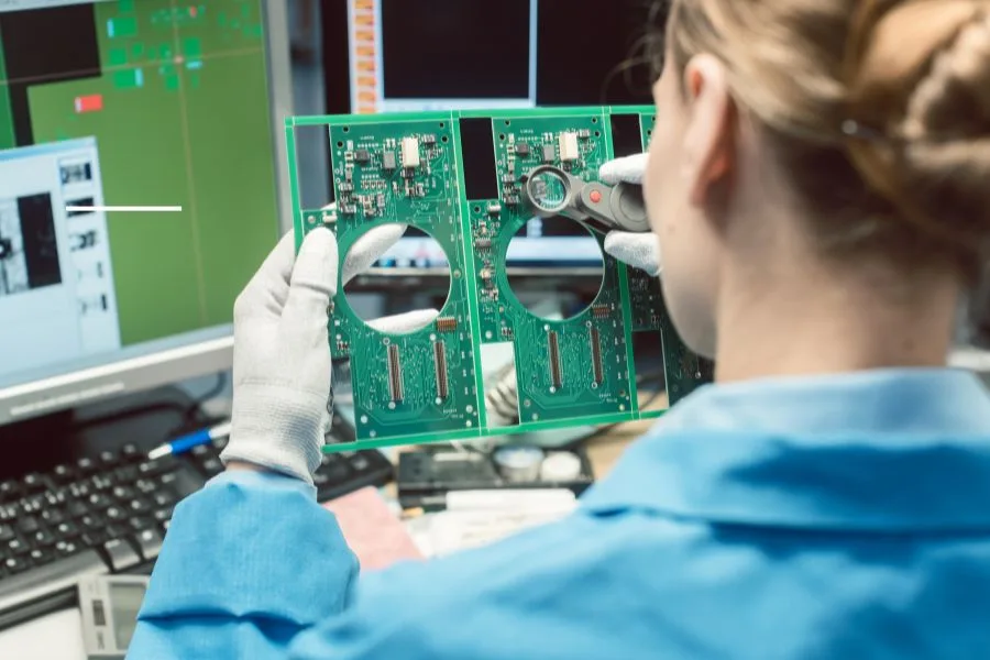
After the etching process, the circuitry is inspected against digital images to ensure it matches the design and is free from defects. Scanning of the board is done initially and then trained inspectors will verify any anomalies that are highlighted in the scanning process. It is important to note that Vonkka PCB does not allow for the repair of open circuits.

Step 8: Lay-up and bond (Lamination)
The inner layers of the PCB undergo a process where an oxide layer is applied and then stacked together with pre-preg acting as insulation between layers. Copper foil is then added to both the top and bottom of the stack. The lamination process involves subjecting the internal layers to high temperature (375 degrees Fahrenheit) and pressure (275 to 400 psi) while laminating with a photosensitive dry resist. After curing at a high temperature, the pressure is gradually released, and the material slowly cooled.

Step 9: Drilling
Next in the PCB production process, holes are drilled to create the electrical connections within the multilayer PCB. This is a mechanical drilling process that must be carefully optimized for precise registration to all of the inner layer connections. The panels can be stacked during this process, and laser drilling is also an option.

Step 10: Chemical & Electroless Copper
The plating process begins with depositing a thin layer of copper on the walls of the holes. This is achieved through a chemical process known as PTH (Plated Through Hole) that results in a reliable deposit of copper even on non-metallic hole walls. While this copper deposit alone is not sufficient, it does provide electrical continuity between layers and through the holes. Following PTH, panel plating is performed to provide a thicker deposit of copper on top of the PTH deposit, typically ranging from 5 to 8 um. This combination of PTH and panel plating optimizes the amount of copper to be plated and etched, meeting the track and gap requirements.

Step 11: Image the Outer Layers
The process for the outer layers is similar to that of the inner layers in terms of image transfer using photosensitive dry film, exposure to UV light, and etching. However, the key difference is that the dry film is removed in areas where copper is desired and where circuitry needs to be defined, enabling the additional plating of copper at a later stage in the process. This step is carried out in a clean room environment.

Step 12: Plating
The next plating stage involves electrolytic plating of additional copper in areas where dry film has been removed to define circuitry. The plating is followed by application of tin to protect the plated copper. This process is also carried out in a clean room environment.

Step 13: Etch Outer Layer
Typically, this process consists of three steps. Initially, the blue dry film is removed, followed by etching away the unwanted copper while the tin deposit acts as an etch resist to protect the necessary copper. Finally, the tin deposit is chemically removed, leaving behind the circuitry.

Step 14: Outer Layer AOI
The panel that has been imaged and etched undergoes a similar AOI process as the inner layer to ensure that the circuitry aligns with the design and is defect-free. PCBWay enforces a strict policy of not allowing any repairs to open circuits.

A layer of soldermask ink is coated onto the entire surface of the PCB. By utilizing artworks and UV light, specific regions are exposed to the UV while the unexposed regions are chemically developed and removed, leaving behind only the areas that are to be utilized as solderable surfaces. The remaining soldermask is then fully cured, resulting in a durable finish. This process is executed within a controlled environment, or clean room.
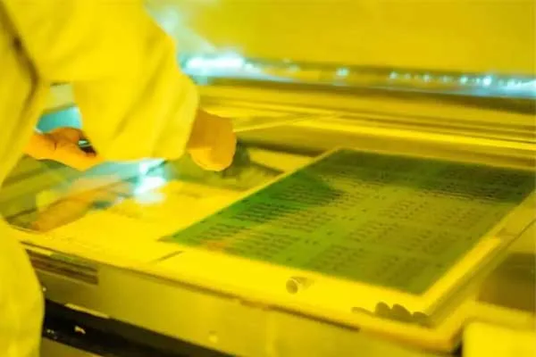
After the completion of the solder mask application, various finishes are added to the exposed copper surfaces. These finishes serve to protect the surface and ensure that the soldering process is efficient. Examples of such finishes include Electroless Nickel Immersion Gold, HASL, and Immersion Silver. It is important to note that thickness measurements and solderability tests are conducted to ensure that the finishes meet the required standards.

Step 17: Electrical Testing
This step is crucial for verifying the quality of the tracks and through hole interconnections to ensure there are no open or short circuits on the final PCB. Two testing methods are used, flying probe for small volumes and fixture-based for larger volumes. Every multilayer PCB is electrically tested against the original board data. Using a flying probe tester, each net is checked to ensure it is complete (no open circuits) and does not short to any other net.

Step 18: Final Inspection
In the final step of the process, a team of highly skilled inspectors conducts a thorough check of each PCB. They visually examine the PCB to ensure that it meets the acceptance criteria, and only PCBWay's "approved" inspectors are entrusted with this task. In addition to manual visual inspection, the team also uses Automated Visual Inspection (AVI) technology, which can quickly compare the PCB to the gerber data with high accuracy, but human verification is still required. All orders undergo a full inspection, including dimensional measurements and solderability tests.

Step 20: Profiling and V-Scoring
Panelizing, or breaking up the manufacturing panels into specific sizes and shapes according to customer design, is the final step of the PCB production process. There are three main methods used for panelizing: scoring, routing, or punching. The dimensions of the panel are measured against the customer's supplied drawing to ensure the panel is the correct size and shape.

Step 21: Packaging
The finished PCBs are carefully wrapped in packaging materials that meet PCBWay's packaging requirements for ESD protection and other standards. They are then placed in boxes according to the customer's shipping preferences, and shipped via the chosen method of transportation.